or


Results for INVENTOR: akram salman AND FULL_TEXT: {akram salman boise id}
Showing 1 – 10 of 651
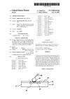
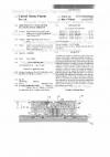
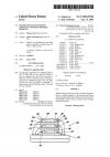
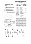
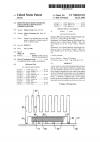
The invention encompasses a board-on-chip package comprising an insulative substrate having circuitry thereon and an opening therethrough. A semiconductive-material-comprising die is adhered to the substrate and electrically connected to the circuitry with a plurality of electrical interconnects extending through the opening. A metal foil is in physical contact with at least a portion of the die. The invention also encompasses a method of forming a plurality of board-on-chip packages. An insulat…
 
An improved wire bond is provided with the bond pads of semiconductor devices and the lead fingers of lead frames or an improved conductive lead of a TAB tape bond with the bond pad of a semiconductor device. More specifically, an improved wire bond is described wherein the bond pad on a surface of the semiconductor device comprises a layer of copper and at least one layer of metal and/or at least a barrier layer of material between the copper layer and one layer of metal on the copper layer to …
 
An electrically conductive apparatus includes, a) an electrically non-conducting substrate, the substrate having a base surface and an adjacent elevated surface, the elevated surface being spaced from the base surface by a first distance thereby defining a step having a step wall; b) a capping layer of first electrically conductive material coating the elevated surface only portions of the step wall, the capping layer having outer top and outer side portions; and c) a conductive trace of second …
 
Exemplary embodiments of the present invention disclose a semiconductor assembly having at least one isolation structure formed. The semiconductor assembly comprises: a first trench in a semiconductive substrate; a second trench extending the overall trench depth in the semiconductive substrate by being aligned to the first trench; and an insulation material substantially filling the first and second trenches. The isolation structure separates a non-continuous surface of a conductive region.
 
An improved inter-metal dielectric structure having a low dielectric constant for reduced capacitive coupling between adjacent metal conductor strips is disclosed. The structure employs silicate glass that is heavily doped with fluorine atoms as the primary dielectric material. The primary dielectric material is encased in an insulative barrier film which has a high degree of impermeability to both fluorine atoms and water molecules. Although the preferred barrier material, silicon nitride, poss…
 
A circuit probing method includes contacting a conductive probe with a contact pad of an electronic circuit. An electric signal is sent between the contacted probe and the contact pad. After sending the signal, the conductive probe and contact pad are removed from contacting one another. After the removing, the conductive probe is chemically cleaned. In a further aspect, an integrated circuit on a semiconductor substrate has at least one conductive contact pad. A circuit probe formed from a semi…
 
Multiple integrated circuit devices in a stacked configuration that use a spacing element for allowing increased device density and increased thermal conduction or heat removal for semiconductor devices and the methods for the stacking thereof are disclosed.
 
A carrier for use in a chip-scale package includes a semiconductor substrate with a plurality of apertures formed therethrough. The apertures of the carrier are aligned with bond pads of a semiconductor device. Conductive material is introduced into each of the apertures of the carrier to form vias therein that establish electrical communication between the bond pads of the semiconductor device and conductive traces that extend to the vias or contacts or conductive structures that are subsequent…
 
Methods relating to singulation of dice from semiconductor wafers. Trenches or channels are formed in the bottom surface of a semiconductor wafer, corresponding in location to wafer streets. The trenches may be formed by etching or through an initial laser cut. The wafer is then singulated along the streets with a laser, preferably having a beam narrower than the trenches. Multiple, laterally spaced lasers may be used in combination during a single pass to perform simultaneous singulating cuts. …
 
A cover, acting as a heat sink for integrated circuit devices, encloses one or more devices mounted on a support structure. The thermally conductive cover is formed of a thermally conductive material and is also sealed to the support structure. By thermally contacting the cover to the integrated circuit devices, heat is dissipated from the integrated circuit devices. A thermally conductive paste can be applied between the cover and integrated circuit devices to facilitate heat transfer from the …
 
1 2 3 4 5 6 7 8 9 10
 
 
About |  FAQs |  Terms & Disclaimer |  Link to Us |  Contact Us